 Multi-band CDMA and WCDMA mobile phones the need for greater RF design work in order to provide sufficient output power and to ensure the linearity and efficiency of the normal operation of each band. Design usually includes a power amplifier and favorable duplex of each frequency band, RF filters and switches to meet the multiple RF input to a single antenna. In order to reduce the multi-band mobile phone design complexity, ANADIGICS硑made a dual-band CDMA and WCDMA power amplifier module. Integrated in a single package through the two power amplifier modules, and before the use of two separate DC and RF power amplifier design of signal lines in comparison, which can effectively reduce the circuit board area. This article will describe the dual-band power amplifier module in the CDMA / EVDO and WCDMA / HSPA mobile phone designed for typical application.
This article will focus on ANADIGICS AWT6221 in UMTS paragraphs 2 and 5-band, dual-band WCDMA / HSPA mobile phone design applications. The AWT6221 has won ANANDIGICS by the Chinese Ministry of Information Industry issued by the application of information technology, communications technology Outstanding Innovation Achievement Award (2) and EDN Innovation Award, communications and network product excellence award.
AWT6221 dual-band power amplifier significantly reduces power consumption up to 75% of the average current, and increase up to 25% of talk time.
ANADIGICS of HELP3™ power amplifier, such as AWT6221 power amplifier uses the company's exclusive InGaP-Plus ™ technology, in the same InGaPGaAs die, which integrates bipolar and field-effect transistor (FET) devices. Through selectable bias modes, HELP3 ™ power amplifier in the low range and mid-range output power levels in the present the best efficiency. Intelligent bias circuit of AWT6221 down at low power levels can be reduced to 8 milliamperes current power - best in the world. By integrating two separate amplifier chains, super-mini AWT6221 in these two frequency bands to provide superior performance, and save the printed circuit board area. (Figure 1)
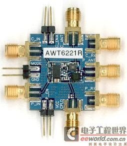
ANADIGICS company is a combination of popular band dual-band WCDMA / HSPA Power Amplifier Module for CDMA / EVDO applications, dual-band power amplifier module. More information can be found ANADIGICS Inc. ANADIGICS company has developed a reference design products to help customers faster, easier to achieve their design goals. In this article we will describe the AWT6221 (Figure 2) reference design advantage. 
 Figure 2. Prototype AWT6221RDA
AWT6221 is a dual-band WCDMA / HSPA mobile UMTS band 2 (824-849MH) and band 5 (1850-1910MHz) and developed. 3GPP technical specification of the user equipment level 3 power, must meet or exceed these minimum performance levels (3)
- Maximum output power: +24 dBm +1 /-3dBm
- Adjacent Channel Leakage Power Ratio (ACLR) + /-5MHz:-33dBm
- Adjacent Channel Leakage Power Ratio (ACLR) + /-10MHz:-43dBm
- Frequency :30–1000MHz:-36dBm/100kHz
- In the between 1-12.75GHz: -30dBm/1MHz
- In the between 869-894MHz: -60dBm/3.84MHz
- In the between 1930-1990MHz: -60dBm/3.84MHz
- In the between 2100-2170MHz: -60dBm/3.84MHz

Describe the N-port S parameters for each one-port network response of the voltage signal. The first number of the subscript refers to the response to mouth, while the second figure refers to the case mouth. S21 refers to the signal side, therefore a result of two reactions in the mouth. S parameters of an equal number of rows and columns from the matrix port. S matrix along the diagonal of the parameters are known as the reflection coefficient, diagonal S parameters are referred to as transmission coefficients, because they only occur in a single port. S matrix of two-port network in the table below:

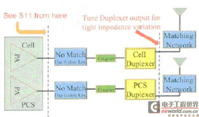
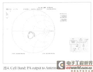
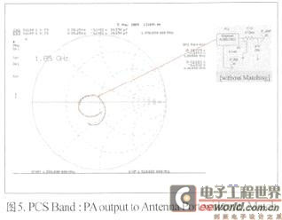
Reflection coefficient (S11) for band 2 and band 5 the frequency range of RF paths to test. Power amplifier at the output of the circuit is not in line with the formation of a series of impedance changes, the results displayed in the Smith form (Figure 4, Figure 5).
 Figure 4. Cell Band: PA output to Antenna
 Figure 5. PCS Band: PA output to Antenna
For any power amplifier, the output impedance have a major impact in the operation, and a strong influence on the transfer to the antenna, linear (ACLR) and operational efficiency of power. ANADIGICS power amplifiers as the vendor can help engineers to do a good job balancing the load-pull of information. Optimum output impedance will be other characteristics of RF chain, the influence of components such as diplexers and switches are not always 50Ω. Variation frequency band characteristics of the advantages of duplex and operating temperature, in well-developed WCDMA RF design, particularly challenging.
0 comments:
Post a Comment